1. Crystal Framework and Layered Anisotropy
1.1 The 2H and 1T Polymorphs: Architectural and Electronic Duality
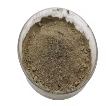
(Molybdenum Disulfide)
Molybdenum disulfide (MoS TWO) is a split shift steel dichalcogenide (TMD) with a chemical formula containing one molybdenum atom sandwiched between 2 sulfur atoms in a trigonal prismatic coordination, developing covalently bonded S– Mo– S sheets.
These specific monolayers are piled vertically and held with each other by weak van der Waals pressures, making it possible for simple interlayer shear and peeling to atomically thin two-dimensional (2D) crystals– an architectural attribute central to its diverse useful duties.
MoS two exists in numerous polymorphic types, one of the most thermodynamically steady being the semiconducting 2H phase (hexagonal symmetry), where each layer exhibits a direct bandgap of ~ 1.8 eV in monolayer type that transitions to an indirect bandgap (~ 1.3 eV) wholesale, a phenomenon crucial for optoelectronic applications.
On the other hand, the metastable 1T phase (tetragonal symmetry) takes on an octahedral sychronisation and behaves as a metal conductor as a result of electron donation from the sulfur atoms, enabling applications in electrocatalysis and conductive compounds.
Phase shifts between 2H and 1T can be induced chemically, electrochemically, or via strain design, supplying a tunable platform for designing multifunctional devices.
The ability to support and pattern these phases spatially within a solitary flake opens pathways for in-plane heterostructures with distinctive electronic domains.
1.2 Defects, Doping, and Side States
The performance of MoS two in catalytic and electronic applications is very conscious atomic-scale flaws and dopants.
Innate point defects such as sulfur jobs serve as electron contributors, increasing n-type conductivity and serving as energetic sites for hydrogen development reactions (HER) in water splitting.
Grain limits and line flaws can either impede fee transportation or develop localized conductive pathways, depending on their atomic configuration.
Controlled doping with transition metals (e.g., Re, Nb) or chalcogens (e.g., Se) allows fine-tuning of the band framework, provider concentration, and spin-orbit combining impacts.
Especially, the sides of MoS ₂ nanosheets, especially the metallic Mo-terminated (10– 10) sides, exhibit substantially greater catalytic activity than the inert basal aircraft, motivating the style of nanostructured catalysts with maximized edge direct exposure.
( Molybdenum Disulfide)
These defect-engineered systems exhibit exactly how atomic-level control can change a naturally occurring mineral into a high-performance useful material.
2. Synthesis and Nanofabrication Techniques
2.1 Bulk and Thin-Film Manufacturing Techniques
Natural molybdenite, the mineral kind of MoS TWO, has actually been utilized for years as a strong lubricant, yet contemporary applications require high-purity, structurally regulated synthetic forms.
Chemical vapor deposition (CVD) is the leading method for generating large-area, high-crystallinity monolayer and few-layer MoS ₂ films on substrates such as SiO TWO/ Si, sapphire, or adaptable polymers.
In CVD, molybdenum and sulfur precursors (e.g., MoO two and S powder) are evaporated at high temperatures (700– 1000 ° C )in control atmospheres, enabling layer-by-layer growth with tunable domain name size and orientation.
Mechanical exfoliation (“scotch tape method”) continues to be a benchmark for research-grade samples, producing ultra-clean monolayers with minimal problems, though it does not have scalability.
Liquid-phase peeling, including sonication or shear mixing of mass crystals in solvents or surfactant solutions, produces colloidal diffusions of few-layer nanosheets ideal for coverings, composites, and ink solutions.
2.2 Heterostructure Assimilation and Gadget Pattern
The true capacity of MoS two emerges when incorporated into vertical or lateral heterostructures with various other 2D materials such as graphene, hexagonal boron nitride (h-BN), or WSe two.
These van der Waals heterostructures make it possible for the style of atomically accurate gadgets, including tunneling transistors, photodetectors, and light-emitting diodes (LEDs), where interlayer charge and energy transfer can be crafted.
Lithographic pattern and etching techniques allow the manufacture of nanoribbons, quantum dots, and field-effect transistors (FETs) with channel lengths down to tens of nanometers.
Dielectric encapsulation with h-BN shields MoS two from environmental destruction and decreases charge spreading, significantly enhancing service provider mobility and tool stability.
These manufacture advances are vital for transitioning MoS two from lab curiosity to feasible component in next-generation nanoelectronics.
3. Useful Properties and Physical Mechanisms
3.1 Tribological Habits and Solid Lubrication
Among the oldest and most long-lasting applications of MoS two is as a dry strong lubricating substance in extreme environments where liquid oils fall short– such as vacuum cleaner, heats, or cryogenic problems.
The low interlayer shear stamina of the van der Waals gap enables simple sliding in between S– Mo– S layers, resulting in a coefficient of rubbing as low as 0.03– 0.06 under optimal conditions.
Its performance is even more enhanced by strong attachment to steel surface areas and resistance to oxidation up to ~ 350 ° C in air, past which MoO two development enhances wear.
MoS two is commonly made use of in aerospace devices, air pump, and weapon elements, commonly applied as a layer through burnishing, sputtering, or composite consolidation into polymer matrices.
Recent research studies reveal that humidity can weaken lubricity by increasing interlayer bond, triggering study right into hydrophobic coatings or hybrid lubricants for better environmental stability.
3.2 Digital and Optoelectronic Reaction
As a direct-gap semiconductor in monolayer kind, MoS two shows strong light-matter interaction, with absorption coefficients going beyond 10 ⁵ centimeters ⁻¹ and high quantum yield in photoluminescence.
This makes it optimal for ultrathin photodetectors with fast response times and broadband sensitivity, from visible to near-infrared wavelengths.
Field-effect transistors based upon monolayer MoS two demonstrate on/off proportions > 10 eight and service provider mobilities approximately 500 cm TWO/ V · s in put on hold samples, though substrate communications commonly limit sensible worths to 1– 20 centimeters ²/ V · s.
Spin-valley combining, an effect of solid spin-orbit interaction and busted inversion symmetry, allows valleytronics– an unique standard for details encoding using the valley level of liberty in momentum room.
These quantum sensations position MoS two as a candidate for low-power reasoning, memory, and quantum computing components.
4. Applications in Energy, Catalysis, and Arising Technologies
4.1 Electrocatalysis for Hydrogen Development Response (HER)
MoS two has emerged as a promising non-precious choice to platinum in the hydrogen evolution reaction (HER), a key procedure in water electrolysis for green hydrogen production.
While the basal plane is catalytically inert, side sites and sulfur jobs display near-optimal hydrogen adsorption free energy (ΔG_H * ≈ 0), equivalent to Pt.
Nanostructuring techniques– such as creating up and down straightened nanosheets, defect-rich movies, or doped hybrids with Ni or Co– take full advantage of active website thickness and electrical conductivity.
When integrated into electrodes with conductive supports like carbon nanotubes or graphene, MoS two achieves high existing thickness and lasting stability under acidic or neutral conditions.
Further improvement is achieved by maintaining the metal 1T stage, which improves intrinsic conductivity and subjects additional energetic websites.
4.2 Versatile Electronic Devices, Sensors, and Quantum Instruments
The mechanical versatility, transparency, and high surface-to-volume ratio of MoS two make it ideal for adaptable and wearable electronic devices.
Transistors, reasoning circuits, and memory tools have been shown on plastic substratums, enabling flexible displays, wellness screens, and IoT sensing units.
MoS TWO-based gas sensing units show high sensitivity to NO TWO, NH THREE, and H ₂ O as a result of charge transfer upon molecular adsorption, with action times in the sub-second variety.
In quantum innovations, MoS ₂ hosts local excitons and trions at cryogenic temperatures, and strain-induced pseudomagnetic fields can trap carriers, allowing single-photon emitters and quantum dots.
These advancements highlight MoS two not just as a practical material yet as a system for exploring basic physics in lowered dimensions.
In recap, molybdenum disulfide exemplifies the merging of classic products scientific research and quantum design.
From its ancient duty as a lubricant to its modern implementation in atomically thin electronics and power systems, MoS ₂ remains to redefine the limits of what is feasible in nanoscale materials style.
As synthesis, characterization, and integration methods advance, its impact throughout science and technology is poised to increase even better.
5. Supplier
TRUNNANO is a globally recognized Molybdenum Disulfide manufacturer and supplier of compounds with more than 12 years of expertise in the highest quality nanomaterials and other chemicals. The company develops a variety of powder materials and chemicals. Provide OEM service. If you need high quality Molybdenum Disulfide, please feel free to contact us. You can click on the product to contact us.
Tags: Molybdenum Disulfide, nano molybdenum disulfide, MoS2
All articles and pictures are from the Internet. If there are any copyright issues, please contact us in time to delete.
Inquiry us