1. Material Principles and Architectural Attributes of Alumina Ceramics
1.1 Crystallographic and Compositional Basis of α-Alumina
(Alumina Ceramic Substrates)
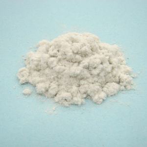
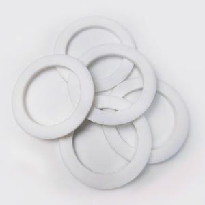
Alumina ceramic substrates, primarily made up of light weight aluminum oxide (Al two O FOUR), work as the backbone of modern-day electronic product packaging because of their remarkable balance of electrical insulation, thermal stability, mechanical strength, and manufacturability.
The most thermodynamically steady phase of alumina at high temperatures is diamond, or α-Al ₂ O FIVE, which takes shape in a hexagonal close-packed oxygen lattice with light weight aluminum ions occupying two-thirds of the octahedral interstitial websites.
This thick atomic arrangement conveys high solidity (Mohs 9), outstanding wear resistance, and solid chemical inertness, making α-alumina appropriate for harsh operating settings.
Industrial substratums typically consist of 90– 99.8% Al ₂ O ₃, with small enhancements of silica (SiO TWO), magnesia (MgO), or unusual planet oxides utilized as sintering help to promote densification and control grain development during high-temperature handling.
Higher pureness qualities (e.g., 99.5% and over) display exceptional electric resistivity and thermal conductivity, while lower purity versions (90– 96%) provide affordable solutions for much less demanding applications.
1.2 Microstructure and Defect Design for Electronic Dependability
The performance of alumina substrates in electronic systems is critically dependent on microstructural uniformity and flaw reduction.
A penalty, equiaxed grain framework– typically varying from 1 to 10 micrometers– guarantees mechanical integrity and decreases the probability of split proliferation under thermal or mechanical stress.
Porosity, specifically interconnected or surface-connected pores, need to be reduced as it degrades both mechanical stamina and dielectric efficiency.
Advanced handling methods such as tape spreading, isostatic pushing, and regulated sintering in air or managed ambiences make it possible for the manufacturing of substratums with near-theoretical density (> 99.5%) and surface roughness listed below 0.5 µm, necessary for thin-film metallization and wire bonding.
Furthermore, contamination segregation at grain borders can lead to leakage currents or electrochemical movement under bias, necessitating strict control over basic material pureness and sintering conditions to ensure long-term reliability in moist or high-voltage atmospheres.
2. Manufacturing Processes and Substratum Manufacture Technologies
( Alumina Ceramic Substrates)
2.1 Tape Spreading and Green Body Processing
The production of alumina ceramic substratums starts with the prep work of a highly dispersed slurry containing submicron Al ₂ O three powder, natural binders, plasticizers, dispersants, and solvents.
This slurry is refined via tape casting– a continuous method where the suspension is spread over a relocating carrier movie making use of a precision physician blade to accomplish consistent density, typically between 0.1 mm and 1.0 mm.
After solvent dissipation, the resulting “environment-friendly tape” is flexible and can be punched, pierced, or laser-cut to create by means of openings for upright interconnections.
Multiple layers may be laminated flooring to develop multilayer substratums for intricate circuit assimilation, although the majority of industrial applications utilize single-layer setups due to set you back and thermal growth considerations.
The eco-friendly tapes are then carefully debound to eliminate organic additives through managed thermal decomposition prior to final sintering.
2.2 Sintering and Metallization for Circuit Combination
Sintering is carried out in air at temperatures between 1550 ° C and 1650 ° C, where solid-state diffusion drives pore removal and grain coarsening to attain complete densification.
The linear shrinking throughout sintering– usually 15– 20%– should be precisely predicted and made up for in the layout of eco-friendly tapes to guarantee dimensional precision of the final substratum.
Complying with sintering, metallization is put on form conductive traces, pads, and vias.
Two key techniques dominate: thick-film printing and thin-film deposition.
In thick-film modern technology, pastes having steel powders (e.g., tungsten, molybdenum, or silver-palladium alloys) are screen-printed onto the substratum and co-fired in a minimizing atmosphere to form durable, high-adhesion conductors.
For high-density or high-frequency applications, thin-film processes such as sputtering or evaporation are utilized to deposit bond layers (e.g., titanium or chromium) followed by copper or gold, making it possible for sub-micron pattern by means of photolithography.
Vias are filled with conductive pastes and terminated to develop electric interconnections in between layers in multilayer designs.
3. Functional Characteristics and Efficiency Metrics in Electronic Solution
3.1 Thermal and Electrical Habits Under Functional Stress
Alumina substrates are valued for their desirable mix of moderate thermal conductivity (20– 35 W/m · K for 96– 99.8% Al Two O TWO), which makes it possible for reliable heat dissipation from power tools, and high quantity resistivity (> 10 ¹⁴ Ω · centimeters), making sure marginal leakage current.
Their dielectric continuous (εᵣ ≈ 9– 10 at 1 MHz) is steady over a broad temperature level and frequency range, making them appropriate for high-frequency circuits as much as numerous ghzs, although lower-κ products like light weight aluminum nitride are favored for mm-wave applications.
The coefficient of thermal development (CTE) of alumina (~ 6.8– 7.2 ppm/K) is sensibly well-matched to that of silicon (~ 3 ppm/K) and certain product packaging alloys, lowering thermo-mechanical anxiety throughout gadget operation and thermal cycling.
Nevertheless, the CTE inequality with silicon stays a problem in flip-chip and straight die-attach configurations, usually calling for certified interposers or underfill products to reduce exhaustion failing.
3.2 Mechanical Robustness and Ecological Longevity
Mechanically, alumina substrates exhibit high flexural strength (300– 400 MPa) and outstanding dimensional security under tons, enabling their usage in ruggedized electronic devices for aerospace, auto, and industrial control systems.
They are resistant to vibration, shock, and creep at elevated temperature levels, keeping structural integrity approximately 1500 ° C in inert atmospheres.
In moist atmospheres, high-purity alumina reveals marginal wetness absorption and outstanding resistance to ion movement, ensuring lasting reliability in outside and high-humidity applications.
Surface hardness also secures against mechanical damage throughout handling and setting up, although treatment has to be taken to prevent side cracking because of integral brittleness.
4. Industrial Applications and Technical Influence Across Sectors
4.1 Power Electronic Devices, RF Modules, and Automotive Equipments
Alumina ceramic substrates are ubiquitous in power electronic modules, including protected entrance bipolar transistors (IGBTs), MOSFETs, and rectifiers, where they supply electric seclusion while promoting warm transfer to warmth sinks.
In radio frequency (RF) and microwave circuits, they serve as carrier systems for crossbreed incorporated circuits (HICs), surface area acoustic wave (SAW) filters, and antenna feed networks due to their stable dielectric properties and reduced loss tangent.
In the auto market, alumina substrates are made use of in engine control devices (ECUs), sensor plans, and electric automobile (EV) power converters, where they withstand heats, thermal biking, and direct exposure to corrosive liquids.
Their integrity under extreme problems makes them essential for safety-critical systems such as anti-lock braking (ABDOMINAL) and advanced vehicle driver support systems (ADAS).
4.2 Medical Devices, Aerospace, and Emerging Micro-Electro-Mechanical Systems
Past consumer and industrial electronics, alumina substrates are employed in implantable clinical tools such as pacemakers and neurostimulators, where hermetic securing and biocompatibility are critical.
In aerospace and protection, they are used in avionics, radar systems, and satellite communication components due to their radiation resistance and stability in vacuum atmospheres.
In addition, alumina is significantly made use of as an architectural and insulating platform in micro-electro-mechanical systems (MEMS), consisting of pressure sensors, accelerometers, and microfluidic gadgets, where its chemical inertness and compatibility with thin-film processing are useful.
As electronic systems remain to demand greater power thickness, miniaturization, and integrity under extreme problems, alumina ceramic substrates stay a cornerstone product, bridging the gap in between performance, cost, and manufacturability in sophisticated digital packaging.
5. Provider
Alumina Technology Co., Ltd focus on the research and development, production and sales of aluminum oxide powder, aluminum oxide products, aluminum oxide crucible, etc., serving the electronics, ceramics, chemical and other industries. Since its establishment in 2005, the company has been committed to providing customers with the best products and services. If you are looking for high quality high alumina castable, please feel free to contact us. (nanotrun@yahoo.com)
Tags: Alumina Ceramic Substrates, Alumina Ceramics, alumina
All articles and pictures are from the Internet. If there are any copyright issues, please contact us in time to delete.
Inquiry us